Unit: AM/FM Stereo Receiver
Manufacturer: JVC
Model: VR-5515X
SN: 11600784
One of my customers rescued this beautiful vintage receiver and brought it for restoration. This is the first time I get this model on my workbench. There is very little information online about this receiver. It looks like this model was initially introduced on the market in 1975. The receiver produces 19.5 watts per channel into 8 ohms with no more than 0.8% total harmonic distortion. I was not able to find a service manual for this receiver. Only a schematic is available online at this time (August 2021) but for slightly different models VR-5515L and VR-5515LX.
Initial Evaluation and Troubleshooting
Besides the common problems related to dirty/oxidized controls this unit also had the issue with the FM tuner. The tuner was tuning each station very well, and the stereo lamp came on as it should. The sound from both channels was crystal clear but after a few minutes, it started crackling. It was pretty noticeable at any volume especially in pauses between songs. The FM tuning needle was also twitching around zero. I decided to check the operating voltages on each transistor in the IF Amplifier circuit (transistors X101 thru X109). The voltage measured on the base, collector, and emitter of each transistor except one and was very close to the reference voltage on the schematic. However, the voltage measured on the base and emitter of transistor X106 was almost double of that on the schematic and fluctuated in a wide range. The original transistor installed in this position is 2SC711. It is not on my list of known transistors prone to failure but there is definitely something wrong with it. A good substitute for 2SC711 is a modern low noise Fairchild KSC1845 transistor. So, I replaced the suspect transistor and measured the operating voltages again. This time the voltage measured on the base, collector, and emitter of X106 was stable and very close to the reference voltages on the schematic. I tested the FM tuner for a while and no crackling sound was detected at any station. The FM tuning needle was also stable without any twitching.
Voltage measured on the base, collector, and emitter of X106 - before and after replacement:
X106, base, schematic: 4.0V
X106, collector, schematic: 13.0V
X106, emitter, schematic: 3.7V
2SC711, base: fluctuating from 8.2 to 8.9V
2SC711, collector: 12.2V
2SC711, emitter: fluctuating from 7.0 to 7.8V
KSC1845, base: 4.1V
KSC1845, collector: 12.3V
KSC1845, emitter: 3.5V
After the issue with the FM tuner was resolved I proceeded with a routine servicing on this unit.
Power Supply & Power Amplifier Board
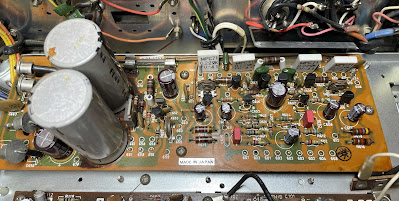
The power supply and power amplifier circuits in this model are all on the same board. It is a pleasure to service this receiver (in comparison to some others) because each PCB has silk lettering on both sides for each electronic component. Not every manufacturer in the 70's followed this rule.
Silk lettering on the back (foil) side of PCB - service friendly receiver
The regulated power supply circuit provides +13V DC for the Tuner, and +20V DC for the Phono, Microphone, and Tone control amplifiers. It also supplies balanced power to the power amplifier from the bridge rectifier and two filter capacitors C627/C628. The circuit has 3 aluminum electrolytic capacitors C651, C654, and C657. I replaced them with low impedance and high-reliability Nichicon UPW/UPM caps. All original e-caps removed from this board were tested with Atlas ESR70 capacitance meter and results are below. All of them are still within the factory capacitance tolerance of +/- 20%.
Test results on original capacitors removed from the power supply circuit:
C651: rated capacitance – 470uF, measured – 531uF, ESR – 0.01Ω, deviation: +13%
C654: rated capacitance – 470uF, measured – 524uF, ESR – 0.01Ω, deviation: +12%
C657: rated capacitance – 470uF, measured – 506uF, ESR – 0.06Ω, deviation: +8%
The power amplifier circuit has eight aluminum e-caps C601/C602, C607/C608, C611/C612, C621, and C622. Two of them (the e-caps C601 and C602) are installed in the signal path. For some reason, regular aluminum electrolytic capacitors were installed in these positions by the manufacturer instead of low leakage e-caps. I think this is a result of a cost reduction strategy by JVC in the middle of 70's. I replaced these two e-caps with high-quality film polyester WIMA MKS2 caps to improve a signal-to-noise ratio. The remaining six e-caps were replaced with low impedance Nichicon UPW/UPM caps. Note, that almost all original e-caps removed from this board are slightly outside of factory capacitance tolerance.
Test results on original capacitors removed from the power amplifier circuit:
C601: rated capacitance – 1uF, measured – 1.24uF, ESR – 1.61Ω, deviation: +24%
C602: rated capacitance – 1uF, measured – 1.24uF, ESR – 1.55Ω, deviation: +24%
C607: rated capacitance – 220uF, measured – 270uF, ESR – 0.11Ω, deviation: +23%
C608: rated capacitance – 220uF, measured – 268uF, ESR – 0.12Ω, deviation: +22%
C611: rated capacitance – 47uF, measured – 51uF, ESR – 0.24Ω, deviation: +9%
C612: rated capacitance – 47uF, measured – 54uF, ESR – 0.18Ω, deviation: +15%
C621: rated capacitance – 220uF, measured – 265uF, ESR – 0.13Ω, deviation: +21%
C622: rated capacitance – 100uF, measured – 127uF, ESR – 0.06Ω, deviation: +27%
Two pre-driver transistors X601 and X602 installed in the power amplifier circuit are notorious 2SA726F transistors. These transistors get very noisy over time. I replaced them with modern low noise Fairchild KSA992 transistors. Watch the pinout on replacement transistors. The original transistor is BCE and the new one is ECB.
According to the schematic, the voltage on pin 660 should be +20V DC. I adjusted it to this value with a trimmer R654.
The voltage on pin 660 was adjusted to +20V DC
Power supply & power amplifier board - before and after
Tone Amplifier Board
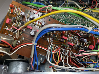
The tone amplifier board has ten aluminum electrolytic capacitors C501/C502, C506, C509/C510, C511/C512, C513/C514, and C525. Four of them C501, C502, C511, and C512 are installed in the signal path. Again, in these positions, the manufacturer installed just ordinary aluminum electrolytic capacitors instead of low leakage e-caps. Actually, I found only one low leakage e-caps and it was installed in the tuner circuit. All other e-caps in this receiver are just regular aluminum capacitors. Anyway, I always replace all e-caps installed in the signal path with either high-quality film polyester caps or low leakage e-caps. This is a crucial step to reduce the noise and improve the performance of any vintage receiver. So, the e-caps C501/C502 were replaced with film polyester WIMA MKS2 caps, and C511/C512 were replaced with low leakage Nichicon UKL caps. The remaining six aluminum e-caps were replaced with low impedance Nichicon UPW caps.
Test results on original capacitors removed from the tone amplifier board:
C501: rated capacitance – 1uF, measured – 1.1uF, ESR – 1.57Ω, deviation: +10%
C502: rated capacitance – 1uF, measured – 1.0uF, ESR – 1.58Ω, deviation: 0%
C506: rated capacitance – 10uF, measured – 13uF, ESR – 1.08Ω, deviation: +30%
C509: rated capacitance – 33uF, measured – 39uF, ESR – 0.78Ω, deviation: +18%
C510: rated capacitance – 33uF, measured – 43uF, ESR – 0.54Ω, deviation: +30%
C511: rated capacitance – 10uF, measured – 11uF, ESR – 0.64Ω, deviation: +10%
C512: rated capacitance – 10uF, measured – 11uF, ESR – 0.58Ω, deviation: +10%
C513: rated capacitance – 10uF, measured – 12uF, ESR – 0.64Ω, deviation: +20%
C514: rated capacitance – 10uF, measured – 11uF, ESR – 0.62Ω, deviation: +10%
C525: rated capacitance – 100uF, measured – 115uF, ESR – 0.19Ω, deviation: +15%
Four NPN transistors (X501 thru X504) installed on this board are notorious 2SC458 transistors. This transistor has different types of failure modes: leakage, noise, and static. I replaced every 2SC458 transistor with a modern low-noise Fairchild KSC1845. Watch the pinout on replacement transistors while servicing this board. The original transistor is BCE and the new one is ECB.
Tone amplifier board - before and after
Phono & Microphone Amplifier Board
The phono and microphone amplifier circuits in this receiver are assembled on the same board. It was quite challenging to work on this PCB since the working space is really very limited. Also, the dial string is located very close to the back (foiled) side of this board and there is a risk of burning the string with a hot soldering iron. It is impossible to remove this board from the chassis without disassembling the front metal panel with a dial string. I didn't want to do it and found a method to overcome it. The front metal panel is mounted on the chassis with four screws on each side. I unscrewed four screws on the right side (close to the variable capacitor) and moved the panel ahead a little bit. It was enough in order to remove the board from the chassis and get much better access for servicing. Be careful at this step while servicing this board. Don't move the front panel too much since there is also a risk to damage a dial string assembly.
Unscrew these four screws on the right side (the 4th screw is hidden on the upper side)
Phono & Microphone amplifier board - removed from the chassis
The microphone amplifier circuit has four aluminum e-caps C431, C435, C436, and C439. Two of them (the e-caps C431 and C436) are installed in the signal path. I replaced them with film polyester WIMA MKS2 caps. The remaining two aluminum e-caps were replaced with low impedance Nichicon UPW caps.
Test results on original capacitors removed from the microphone amplifier circuit:
C431: rated capacitance – 1uF, measured – 1uF, ESR – 1.57Ω, deviation: 0%
C435: rated capacitance – 33uF, measured – 42uF, ESR – 0.64Ω, deviation: +27%
C436: rated capacitance – 1uF, measured – 1uF, ESR – 1.77Ω, deviation: 0%
C439: rated capacitance – 100uF, measured – 112uF, ESR – 0.15Ω, deviation: +12%
This board has a bunch of notorious 2SC458 transistors. Two of them X431 and X432 are installed in the microphone circuit. And four X401 thru X404 are installed in the phono circuit. I replaced each 2SC458 transistor with a modern low noise Fairchild KSC1845. Again, pay attention to the pinout on replacement transistors while servicing this board.
The phono amplifier board has nine aluminum e-caps C401/C402, C409/C410, C413/C414, C419, and C425/C426. Four of them C401/C402 and C413/C414 are installed in the signal path. I replaced them with film polyester WIMA MKS2 caps. The other five aluminum e-caps were replaced with low impedance Nichicon UPW caps.
Test results on original capacitors removed from the phono amplifier circuit:
C401: rated capacitance – 1uF, measured – 1.1uF, ESR – 1.58Ω, deviation: +10%
C402: rated capacitance – 1F, measured – 1.1uF, ESR – 1.72Ω, deviation: +10%
C409: rated capacitance – 10uF, measured – 12uF, ESR – 1.46Ω, deviation: +20%
C410: rated capacitance – 10uF, measured – 12uF, ESR – 1.44Ω, deviation: +20%
C413: rated capacitance – 1uF, measured – 1.1uF, ESR – 1.75Ω, deviation: +10%
C414: rated capacitance – 1uF, measured – 1.1uF, ESR – 1.63Ω, deviation: +10%
C419: rated capacitance – 220uF, measured – 242uF, ESR – 0.11Ω, deviation: +10%
C425: rated capacitance – 10uF, measured – 11uF, ESR – 1.56Ω, deviation: +10%
C426: rated capacitance – 10uF, measured – 12uF, ESR – 1.43Ω, deviation: +20%
Phono & Microphone amplifier board - before and after
Dial and Meter Lamps
It is pretty simple to replace the dial bulbs on this model. One just needs to straighten four metal petals and release the long narrow PCB holding four dial bulbs. I replaced the original bulbs with new incandescent lamps.
Long narrow PCB holding four dial bulbs - just straighten four metal petals to release it
New dial bulbs installed
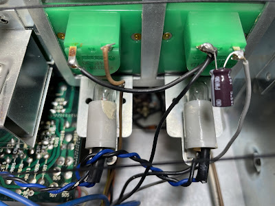
The signal and tuning meter lamps can be replaced even easier than the dial lamps. I also replaced the e-cap C55 across the meter leads with a new Nichicon UPW cap.
Signal and tuning meter bulbs - original and new
Idling Current Adjustment
As I mentioned earlier I didn't find the service manual for this model. The typical idling current is usually ranging from ~20 to 30mA. It is controlled with trimmers R619 (left channel) and R620 (right channel) on this model. The resistance of each emitter resistor is 0.22Ω. Therefore, the voltage across each emitter resistor should be ~4.4mV (0.02A x 0.22Ω = 0.0044V). I adjusted it to ~5mV on each channel. It roughly corresponds to an idling current of 23mA.
Idling current adjustments on the left and right channel
Output Power Test
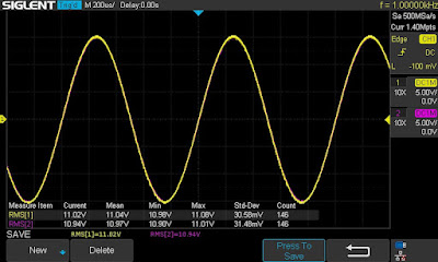
At the end of my restoration, I loaded this receiver with a low inductance 8Ω/100W dummy resistor for each channel, connected my oscilloscope across the speaker terminals, and applied a sine-wave signal of 1kHz to the AUX jacks. The output sine-wave signal was perfectly symmetrical on both channels with no clipping up to 11.02 VRMS (left channel) and 10.94 VRMS (right channel). It corresponds to the output power of 15.2W on the left channel and 15.0W on the right channel.
Output power test
As usual, all the knobs and the front panel were gently cleaned in warm water with dish soap. All controls have been cleaned with DeoxIT 5% contact cleaner and lubricated with DeoxIT FaderLube 5% spray.
All issues with electronics have been solved and the receiver works normally again. The final result can be seen in the photos below. Please watch a short demo video at the end of this post. Thank you for reading.
JVC VR-5515X - after restoration


I found a “warranty card” for this receiver that my dad purchased on 12/23/74 from a Radio Shack in Ithaca, NY. Must’ve been a Xmas gift for the family. 😊 I remember it fondly!
ReplyDeleteI have a large tuner amplifier about the same vintage, I purchased it brand new in 1974. It' a discrete 4 channel 4VR-5456X. It has an inbuilt CD4 demodulator in it. I have always been a bit disappointed with the cleaniness of the amplifier section. The left channel has always had a niticeable hiss in it. At the time I checked out other reviews of the same amp and they were all the same. I also have a very powerfull Marantz amp and pre amp and it is so much cleaner. I have not used the JVC for a few years but intend to restore it and get it up and running again. I matched the JVC with a JL-B44 direct drive turntable which I modified and put on a SME 3009 series 2 tone arm. I also used an Audio Technica AT20sla cartridge with the SME (shibata stylus). I still some CD4 4 channel records and the original JVC setup record for the discrete 4 channel.
ReplyDeleteWow wery dood job
ReplyDeleteExcellent work and very usefull description! Thank you for sharing. I'm also working on restoring a similar model (VR-5535X), must be very close (Judging from the pictures and components). Mine suffers periodicaly from one channel audio - I suspect the driver transistors as well....we'll see. Thanks again :)
ReplyDeleteNice work. I'm waking up a 40 year dormant JVC VR5506, and discovered the tuning dial string is slipping. Will attempt to replace.
ReplyDelete